PLECS Spice is finally here.
Written together with Riccardo Breda, Power Electronics Engineer
PLECS Spice brings SPICE device-level simulation directly into PLECS. Available with PLECS 5.0, both system-level and device-level analysis can be performed within a single tool, eliminating the need to maintain duplicate models across separate softwares.
Separate Tools, Duplicate Work
Power electronics design has long faced a fundamental trade-off: system-level simulation tools deliver the speed and robustness needed for controller development and overall system analysis, but sacrifice the device-level detail necessary to validate component selection before procurement.
For over 20 years, Plexim has promoted a top-down design philosophy, enabling engineers to model complete power electronic systems using ideal switches and behavioral components. By avoiding the computational burden of simulating detailed switching transients, PLECS enables rapid validation of system-level requirements like efficiency, control performance and thermal behavior.
Conversely, traditional SPICE simulators embody an inherently bottom-up approach. They excel at validating device-level requirements through detailed semiconductor models, capturing switching losses, voltage overshoots and parasitic effects with high fidelity. This comes at a cost: system-level integration becomes computationally prohibitive.
This divide has forced engineers into parallel workflows using separate software platforms with different modeling approaches and incompatible component libraries. Moving from a system-level PLECS model to SPICE for device validation requires recreating the model, an error-prone and time-consuming process.
PLECS Spice
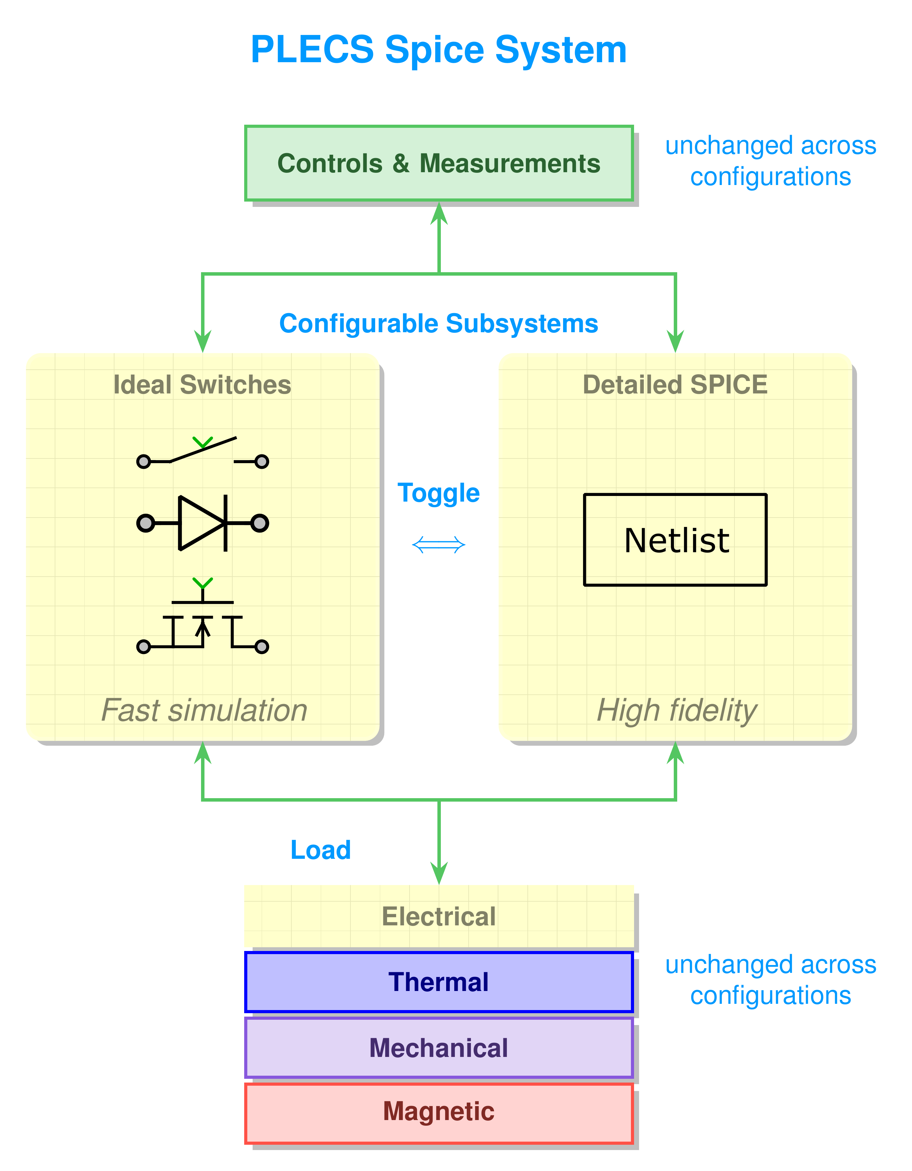
To solve this problem, Plexim has developed PLECS Spice, an extension that brings SPICE device-level simulation capabilities directly into PLECS. PLECS Spice can simulate hybrid systems containing both standard PLECS and SPICE circuits. This allows a schematic to be progressively refined by replacing the ideal switches in a circuit of interest, like the power stage, with detailed SPICE netlists. Controls and other subsystems can remain unchanged. Because the entire workflow stays within PLECS, engineers can easily toggle between ideal and detailed configurations to compare results. This creates a true top-down workflow where device-level detail is added selectively, only where needed. With PLECS Spice, there is no longer a need to build the same model twice.
Under the Hood
The PLECS Spice extension adds four key ingredients that transform PLECS into a fully-featured hybrid simulation platform that can simulate standard PLECS and SPICE models together.
Netlist Parser
SPICE models are typically distributed as netlists. Simply put, these are text files that describe a circuit topology, component interconnections and parameter values. A key capability of PLECS Spice is its parser’s support for multiple netlist dialects. Different SPICE implementations use distinct syntax conventions, making netlists from various vendors incompatible. The PLECS Spice parser handles these variations automatically, enabling engineers to integrate models provided by different semiconductor manufacturers directly into their schematics. Little to no manual conversion or syntax adaptation is needed, regardless of the dialect.
Compact Models
Netlists provided by manufacturers often rely on well-established semiconductor device models. These compact models combine physics-based modeling with empirical corrections to capture fundamental electrical behavior while maintaining reasonable complexity. PLECS Spice includes optimized implementations of compact models such as diodes, MOSFETs, BJTs, and switches. Each model defines a set of parameters that can be tuned to match the electrical response of specific physical devices. In PLECS Spice, classical compact models have been improved to guarantee continuity of key physical quantities, enhancing numerical stability. By tightly integrating these models into the solver, PLECS Spice achieves both computational efficiency and robust convergence even in the presence of highly nonlinear semiconductor characteristics.
Modified Nodal Analysis
Standard PLECS uses piecewise state-space equations to simulate electrical models. This approach is computationally efficient for circuits with mostly linear components but struggles with the strong nonlinearities present in detailed semiconductor models. To handle these nonlinearities, SPICE uses Modified Nodal Analysis (MNA), a formulation that produces differential algebraic equations (DAEs).
MNA constructs the circuit equations by applying Kirchhoff’s current law at each node and substituting component branch equations. Energy storage elements introduce differential equations, while the network topology and sources introduce algebraic constraints. The result is a coupled system where nodal voltages, source currents, and energy storage currents must satisfy both differential and algebraic equations simultaneously. This integrated treatment of constraints and dynamics is what makes MNA particularly robust for nonlinear semiconductor models.
Mixed-Formulation Solver
PLECS Spice employs third-order implicit Runge-Kutta methods augmented with circuit-tailored convergence helpers to solve the DAEs produced by MNA. These one-step methods have a crucial advantage for mixed-signal schematics that contain both SPICE and standard PLECS electrical circuits: they are inherently self-starting. In other words, they do not rely on information from previous time steps. When events such as topology changes or zero-crossings occur, the solver must compute the next time step using only the current state. This self-starting property makes one-step methods particularly well-suited for hybrid systems with frequent discontinuities.
The solver can simulate complex systems that combine standard PLECS and SPICE models in a single schematic. The only rule is that when an electrical circuit contains a netlist, it must be solved using MNA, and therefore all its components must be compatible with SPICE. But other electrical circuits can remain in the standard PLECS formulation. Circuits of different types connect through the control domain, for example using sources and meters or variable capacitances/inductances. This enables a powerful top-down workflow: engineers can refine specific circuits of interest by converting them to SPICE netlists while keeping other subsystems and controls unchanged in standard PLECS.
Application Example
Mixed-signal simulation is particularly valuable when control strategies and device physics must be considered together. The soft switching operation of a Dual Active Bridge (DAB) converter, whose analysis requires taking into consideration both controls and circuit design aspects, serves as a perfect case study for the workflow enabled by PLECS Spice.
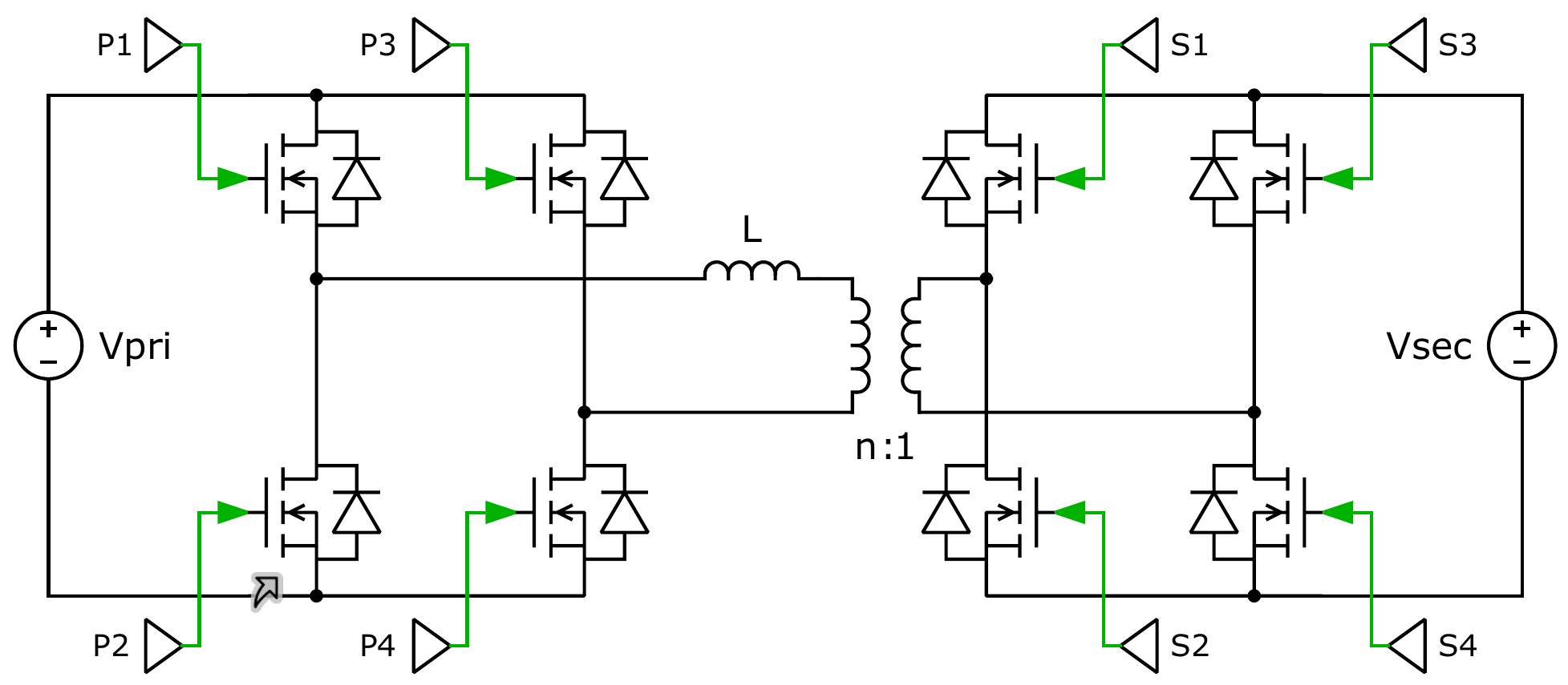
A DAB is a bidirectional DC-DC topology comprising identical primary and secondary bridges (typically full bridges) separated by a high-frequency transformer and an energy transfer inductance (representing leakage plus external inductance). It is widely employed in high-power, high-density applications requiring bidirectional power flow between two galvanically isolated sides, such as EV chargers and energy storage systems.
The Soft Switching Challenge
Magnetic components are often the primary limitation to increasing power density. Their size can be reduced by increasing switching frequency. State-of-the-art designs have reached the hundreds of kHz range. However, at these frequencies, switching losses represent a significant part of the overall converter losses. Without careful design, the volume advantage of a smaller transformer could be negated by the increased size needed of the cooling system.
To resolve this dilemma, soft switching offers a compelling solution. Given the high switching frequencies, MOSFETs are the standard choice for modern DABs. However, their dominant loss mechanism stems from the charge stored in the parasitic output capacitance (). When the device blocks voltage, this capacitance stores the energy
which depends on the drain-source voltage. When a MOSFET is turned on, the stored charge must be evacuated. In hard switching, the closing channel effectively shorts the capacitance, dissipating the stored energy as heat within the semiconductor. At high frequencies, this thermal penalty becomes unsustainable.
Here, the DAB offers a distinct advantage. In a full-bridge topology, each leg contains a top and bottom switch that operate complementarily: when one conducts, the other blocks. In practice, a short interval called dead time is introduced between turning off one switch and turning on its complement. Its primary role is to prevent a short circuit across the DC link, but a DAB can also exploit this interval of time for soft switching. During dead time, the inductor current continues to flow. With both switches off, the only path available is through the parasitic capacitances. This discharges the output capacitance of the incoming MOSFET (the switch about to turn on), causing its drain-source voltage to fall. If the dead time is sufficient, reaches zero before the gate signal arrives. The soft switching challenge lies in properly tuning this interval.
To achieve such Zero Voltage Switching (ZVS), the relationship between the device output capacitance, the resonant path and the gate drive, must be carefully adjusted. Crucially, these hardware choices cannot be made in isolation. They must inform the control design. This is because robust ZVS depends on several dynamic factors: the converter’s operating point (voltage and power), the gate driving scheme (specifically the dead times) and the degrees of freedom utilized by the modulation strategy.
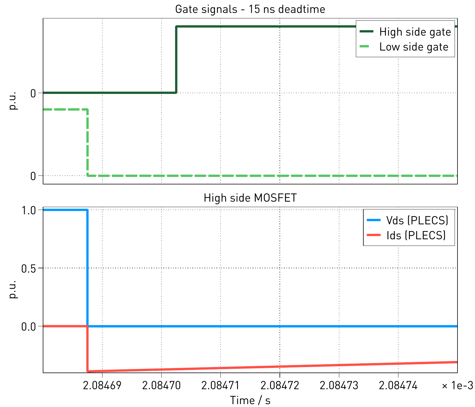
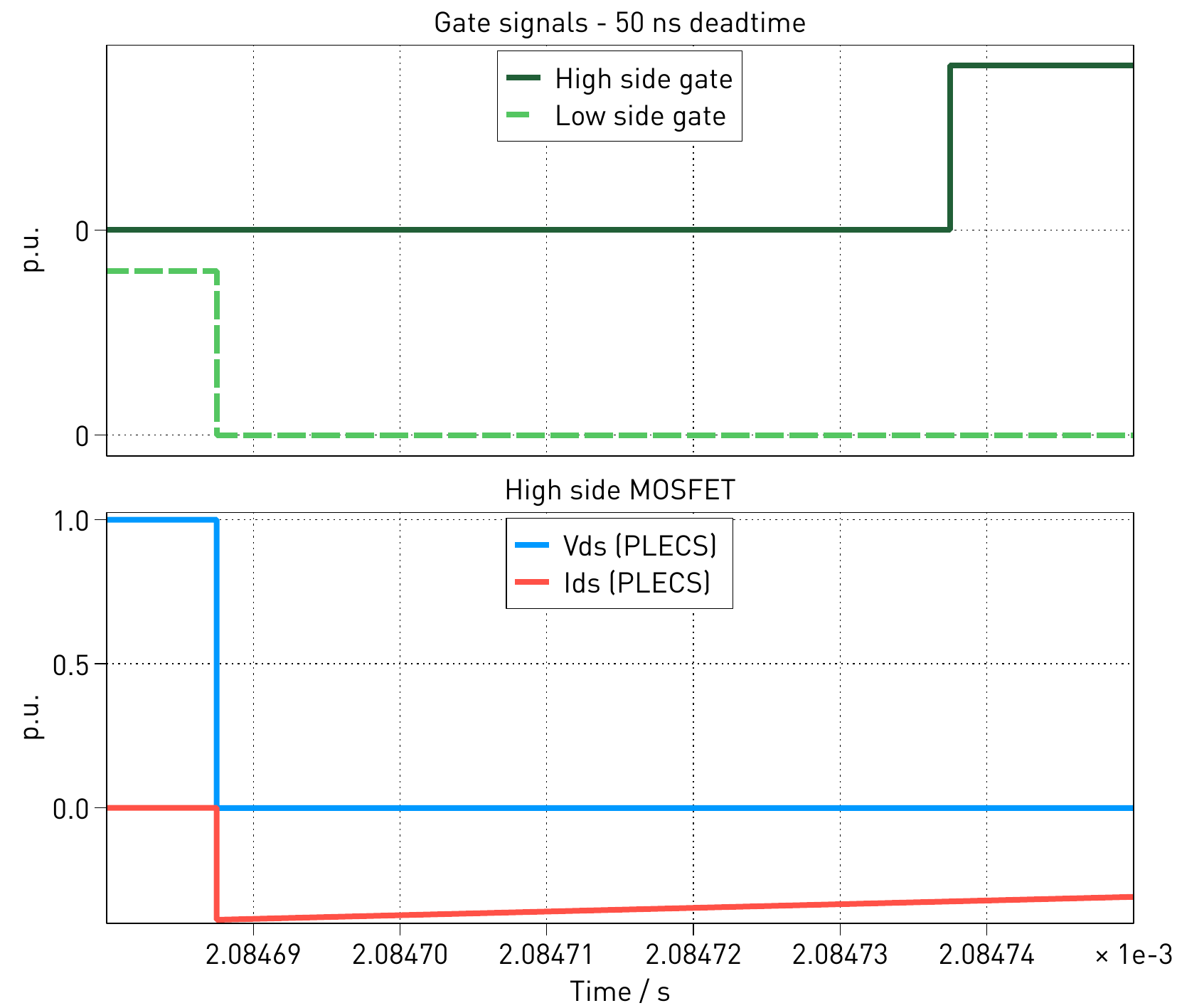
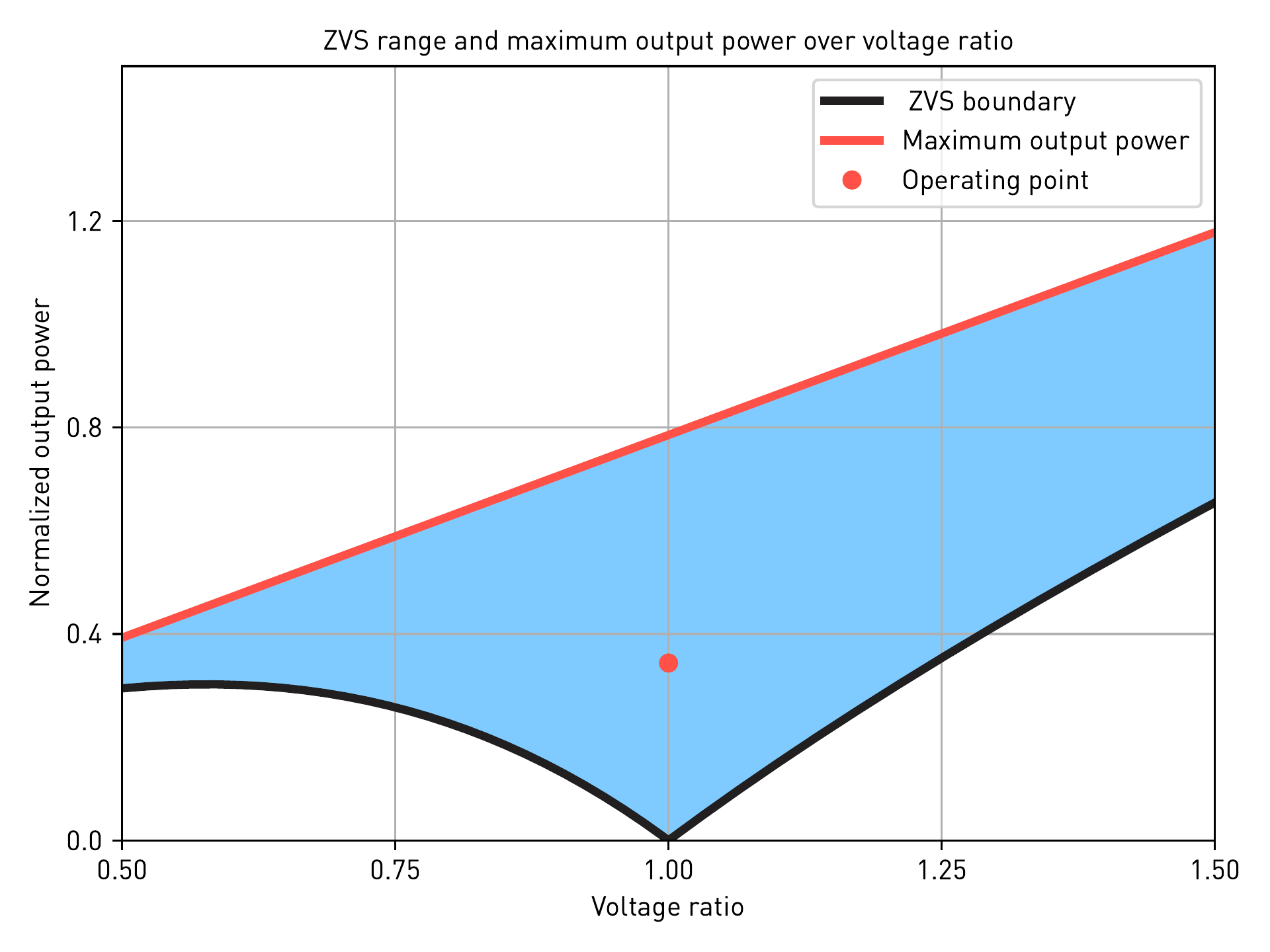
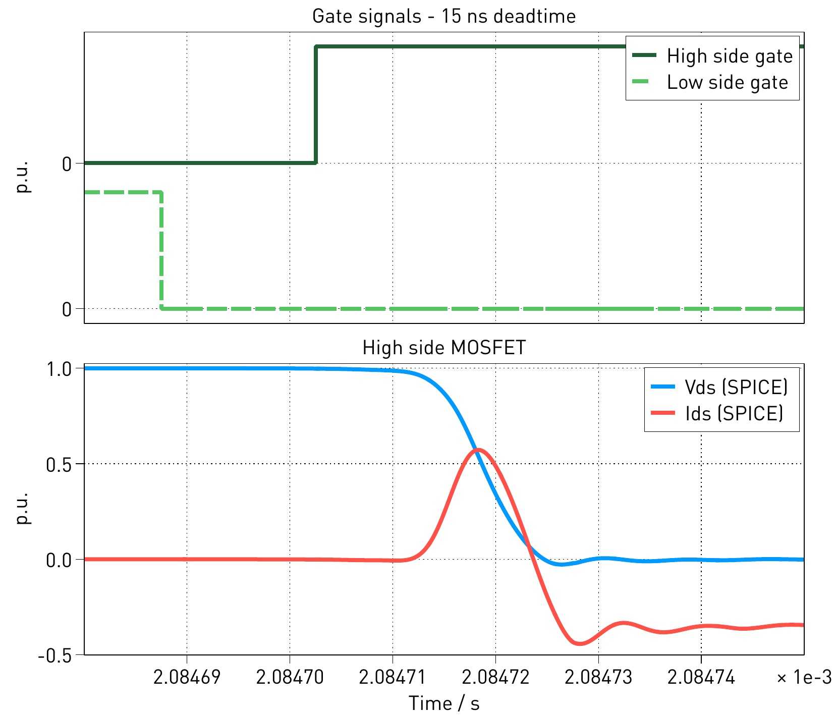
Standard PLECS simulations allow for precise tuning of the operating point within the ZVS region, represented by the blue area in the ZVS range figure. However, because ideal switches are inherently hard switching, they do not simulate the transients required for a detailed analysis of ZVS. The effects of using two different dead times are compared in the figures above. In both tests, the low side gate signal turns off a conducting MOSFET. After the dead time, the complementary MOSFET is turned on by the high side gate signal. In the first experiment, a dead time of 15 ns is used between the two events. In the second, it is set to 50 ns. Yet, the resulting voltage and current waveforms show no visible response to this parameter change.
In this case, the ideal model fails to indicate whether the timing achieves soft switching or leads to hard switching transients. The reason is that ideal switches lack parasitic capacitances. Without , the antiparallel diode of the complementary switch conducts immediately, making the simulated waveforms insensitive to the dead time.
Validating ZVS with Device-Level Detail
PLECS Spice enables precisely the analysis that ideal models cannot provide. Using configurable subsystems, engineers can add a detailed SPICE configuration alongside the ideal model, allowing them to toggle between fast system-level analysis and high-fidelity device validation without modifying the circuit topology or control logic.
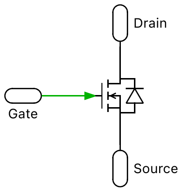
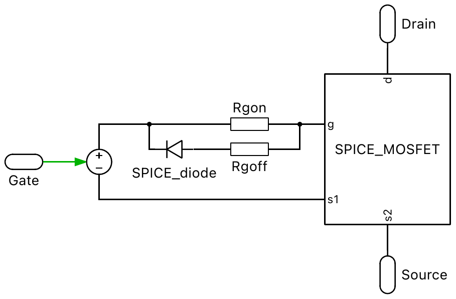
The ideal switch configuration shown in the first figure consists of a standard PLECS MOSFET with antiparallel diode, driven directly by a control signal. The detailed configuration in the second figure provides a device-level description. It uses manufacturer-provided MOSFET and diode netlists that capture parasitic capacitances and charge dynamics. The control signal is converted to a gate-source voltage through a controlled voltage source. Separate on and off gate resistances ( and ) control switching speed. Engineers can switch between one configuration to the other between two simulations, while the control logic, operating point and all other subsystems remain unchanged.
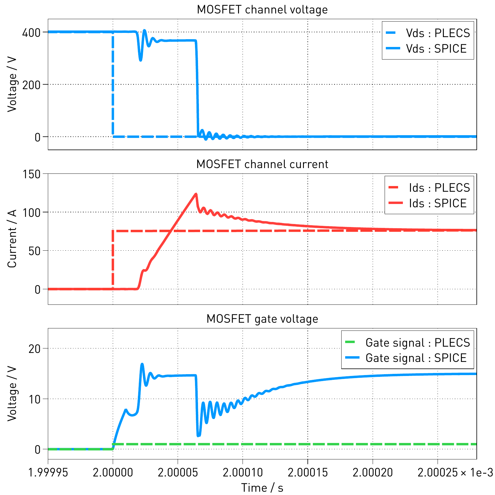
With detailed device models in place, the impact of dead time on ZVS becomes immediately visible. The figure below shows the switching transient with a 15 ns dead time. The drain-source voltage remains high when the gate signal is applied, and only begins falling as channel current rises. This overlap between voltage and current is the signature of hard switching: the channel conducts before the output capacitance fully discharges, dissipating the stored energy as heat in the semiconductor. The insufficient dead time prevents the resonant discharge mechanism from completing.
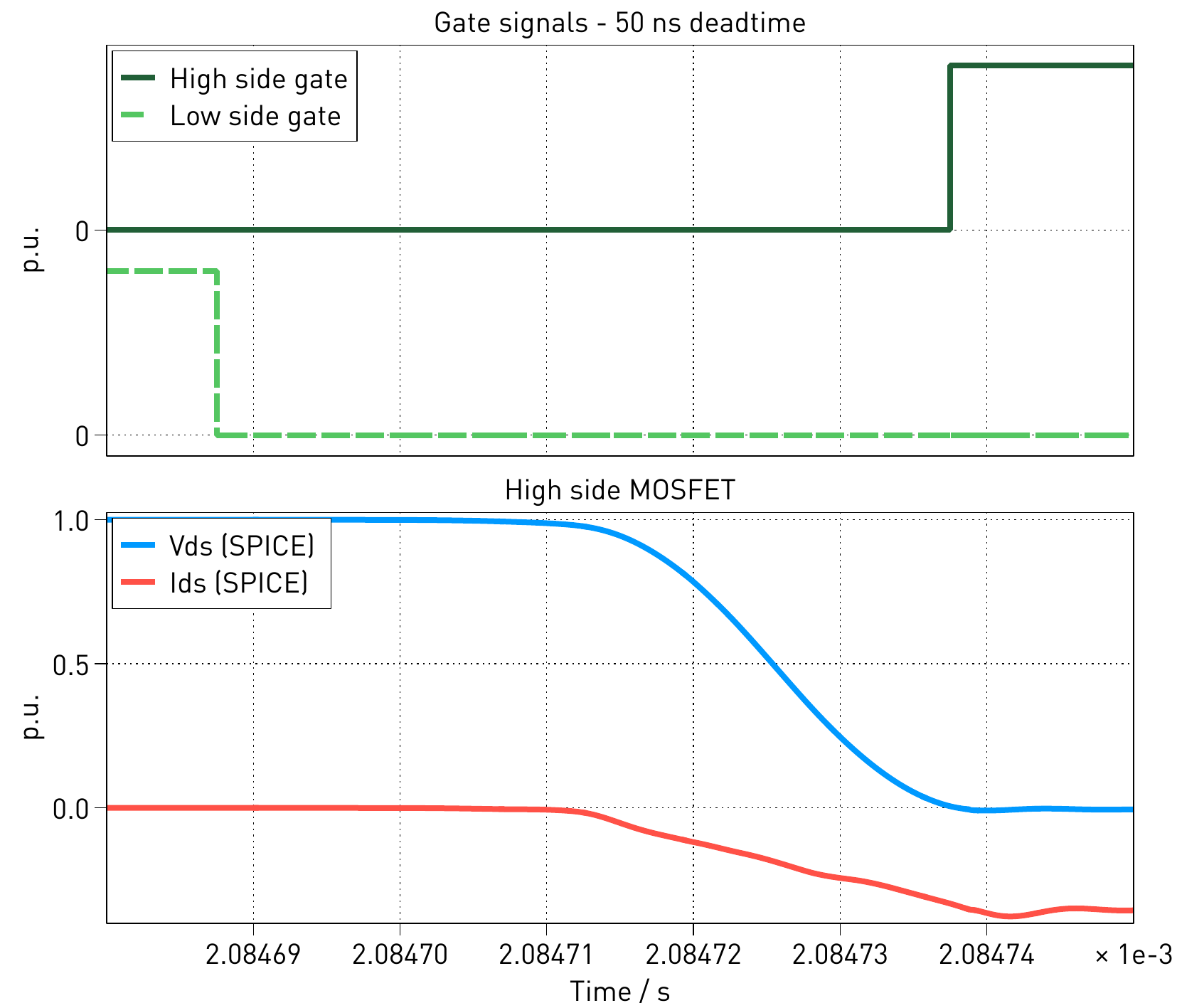
By contrast, the second figure demonstrates successful ZVS with a 50 ns dead time. Here, completes its resonant transition to zero before the gate signal arrives. The channel opens with zero voltage across it, eliminating capacitive turn-on losses. Channel current then begins to flow, carrying the inductor current through the device. This extended dead time provides a sufficient interval for the inductor current to transfer energy from the MOSFET’s output capacitance, fulfilling the conditions for soft switching.
This example demonstrates how PLECS Spice enables validation of ZVS by bringing together three tightly coupled aspects within a single model. The control strategy establishes the operating point and determines the available inductor current for resonant transitions. Gate drive timing sets the window for capacitor discharge. The device physics, captured in the SPICE netlist, determines how quickly that discharge occurs.
Conclusion
PLECS Spice marks a significant step towards a unified power electronics design workflow. By integrating SPICE simulation directly into the PLECS environment, engineers no longer need to choose between system-level insights and device-level accuracy. The ability to seamlessly transition between ideal and detailed models within a single schematic eliminates the redundant and error-prone process of rebuilding circuits in separate tools. This empowers engineers to adopt a true top-down design philosophy, starting with a system-level view and progressively adding detail where it matters most. As power electronic systems grow in complexity, this unified approach will be crucial for accelerating innovation and reducing time-to-market.